Subscribe to EDOM TECH Newsletter
ROHM
2019/08/05
New Ultra-Compact Automotive-Grade MOSFETs Provide Superior Mounting Reliability

Enable greater miniaturization in automotive devices such as ADAS camera modules
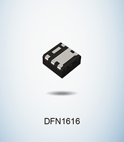
ROHM today announced the development of ultra-compact 1.6x1.6mm size MOSFETs that deliver superior mounting reliability. The RV4xxx series is AEC-Q101 qualified, ensuring automotive-grade reliability and performance under extreme conditions. ROHM’s original package processing technology enables the miniaturization of automotive components, such as ADAS camera modules, that demand high quality.
In recent years, the growing number of vehicle safety and convenience systems such as ADAS cameras has emphasized the challenge of limited space to accommodate these systems, and spurring the demand for smaller components. To meet this need, bottom electrode type MOSFETs that can be miniaturized while maintaining high current are increasingly attracting attention.
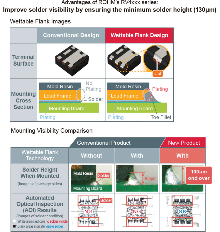
However, for automotive applications optical inspection is performed during the assembly process to ensure quality, but in the case of bottom electrode components solder height cannot be verified after mounting, making it difficult to confirm mounting conditions.
ROHM has a proven track record of developing and introducing new products ahead of market trends, and such is the case with the new ultra-compact MOSFETs. This time, ROHM has become the first in the industry to ensure the minimum solder height (130μm) required for vehicle applications by utilizing original Wettable Flank formation technology. The result is a consistent solder quality – even for compact products – enabling automatic inspection machines to easily verify solder conditions after mounting.
ROHM is committed to developing compact products that leverage this technology, including bipolar transistors and diodes, allowing us to expand our extensive product portfolio and achieve greater miniaturization while providing higher reliability.

Key Features
1. Proprietary Wettable Flank technology guarantees a minimum solderROHM’s Wettable Flank formation technology involves making a step cut into the lead frame on the side of the package before plating. However, burrs resulting from cutting into the lead frame can occur more frequently as the height of the step cut increases.
In response, ROHM developed a unique method that introduces a barrier layer on the entire surface of the lead frame to minimize the occurrence of burrs. This not only prevents component rise and solder defects during mounting, but is the first on the market to ensure a minimum solder height of 130μm for DFN1616 (1.6x1.6mm) packages.

2. Contributes to longer application operation by reducing standby current consumption
Until recently, Schottky barrier diodes (SBDs) were commonly used in the reverse connection protection circuits of ADAS camera modules. But due to the larger currents required by high resolution cameras in advanced vehicle systems, SBDs are increasingly being replaced by compact MOSFETs that provide low ON resistance and less heat generation. For example, at a current and power consumption of 2.0A and 0.6W, respectively, conventional automotive MOSFETs can reduce mounting area by 30% over SBDs. However, adopting bottom electrode MOSFETs capable of providing excellent heat dissipation while still supporting large currents in an even smaller form factor makes it possible to decrease mounting area by as much as 78% compared with conventional SBDs.
Terminology
Automated Optical Inspection (AOI)Commonly used at manufacturing sites to perform automated visual inspection of printed circuit boards and the like. AOI involves scanning boards with a camera to inspect for missing components or quality defects.
Wettable Flank Technology
A technique that makes a step cut into the lead frame on the side of bottom electrode packages such as QFN and DFN before plating. This increases the solder joint surface between the package and substrate, improving solder wettability to allow easy verification of solder condition after mounting.


